


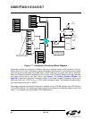
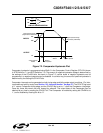
C8051F340/1/2/3/4/5/6/7
56 Rev. 0.5
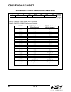
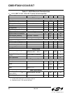
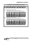
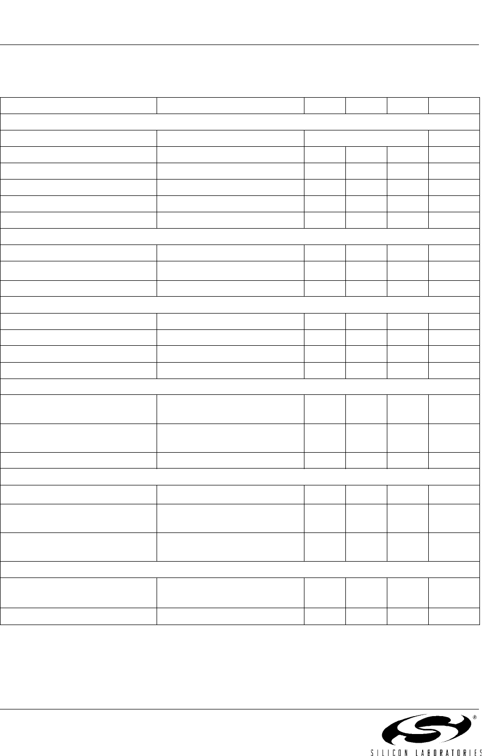
Table 5.1. ADC0 Electrical Characteristics
V
DD
= 3.0 V, VREF = 2.40 V, –40 to +85 °C unless otherwise specified
Parameter Conditions Min Typ Max Units
DC Accuracy
Resolution 10 bits
Integral Nonlinearity ±0.5 ±1 LSB
Differential Nonlinearity Guaranteed Monotonic ±0.5 ±1 LSB
Offset Error 0 LSB
Full Scale Error -1 LSB
Offset Temperature Coefficient 10 ppm/°C
Dynamic Performance (10 kHz sine-wave Single-ended input, 1 dB below Full Scale, 200 ksps)
Signal-to-Noise Plus Distortion 51 52.5 dB
Total Harmonic Distortion
Up to the 5
th
harmonic
–67 dB
Spurious-Free Dynamic Range 78 dB
Conversion Rate
SAR Conversion Clock 3 MHz
Conversion Time in SAR Clocks 10 clocks
Track/Hold Acquisition Time 300 ns
Throughput Rate 200 ksps
Analog Inputs
ADC Input Voltage Range Single Ended (AIN+ – GND)
Differential (AIN+ – AIN–)
0
–VREF
VREF
VREF
V
V
Absolute Pin Voltage with respect
to GND
Single Ended or Differential 0
V
DD
V
Input Capacitance 5 pF
Temperature Sensor
Linearity
1
±0.1 °C
Slope
2
TBD
±TBD
mV / °C
Offset
1,2
(Temp = 0 °C)
TBD
±TBD
mV
Power Specifications
Power Supply Current (V
DD
sup-
plied to ADC0)
Operating Mode, 200 ksps 400 900 µA
Power Supply Rejection ±0.3 mV/V
Notes:
1. Includes ADC offset, gain, and linearity variations.
2. Represents mean ± one standard deviation.