


C8051F340/1/2/3/4/5/6/7
154 Rev. 0.5
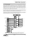
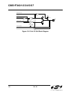
15.3. General Purpose Port I/O
Port pins that remain unassigned by the Crossbar and are not used by analog peripherals can be used for
general purpose I/O. Ports 3-0 are accessed through corresponding special function registers (SFRs) that
are both byte addressable and bit addressable. Port 4 (C8051F340/1/4/5 only) uses an SFR which is
byte-addressable. When writing to a Port, the value written to the SFR is latched to maintain the output
data value at each pin. When reading, the logic levels of the Port's input pins are returned regardless of the
XBRn settings (i.e., even when the pin is assigned to another signal by the Crossbar, the Port register can
always read its corresponding Port I/O pin). The exception to this is the execution of the read-modify-write
instructions. The read-modify-write instructions when operating on a Port SFR are the following: ANL,
ORL, XRL, JBC, CPL, INC, DEC, DJNZ and MOV, CLR or SETB, when the destination is an individual bit
in a Port SFR. For these instructions, the value of the register (not the pin) is read, modified, and written
back to the SFR.
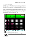
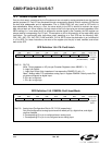
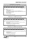
SFR Definition 15.4. P0: Port0 Latch
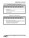
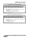
SFR Definition 15.5. P0MDIN: Port0 Input Mode
Bits7–0: P0.[7:0]
Write - Output appears on I/O pins per Crossbar Registers (when XBARE = ‘1’).
0: Logic Low Output.
1: Logic High Output (high impedance if corresponding P0MDOUT.n bit = 0).
Read - Always reads ‘0’ if selected as analog input in register P0MDIN. Directly reads Port
pin when configured as digital input.
0: P0.n pin is logic low.
1: P0.n pin is logic high.
R/W R/W R/W R/W R/W R/W R/W R/W Reset Value
P0.7 P0.6 P0.5 P0.4 P0.3 P0.2 P0.1 P0.0 11111111
Bit7 Bit6 Bit5 Bit4 Bit3 Bit2 Bit1 Bit0 SFR Address:
(bit addressable)
0x80
Bits7–0: Analog Input Configuration Bits for P0.7–P0.0 (respectively).
Port pins configured as analog inputs have their weak pull-up, digital driver, and digital
receiver disabled.
0: Corresponding P0.n pin is configured as an analog input.
1: Corresponding P0.n pin is not configured as an analog input.
R/W R/W R/W R/W R/W R/W R/W R/W Reset Value
11111111
Bit7 Bit6 Bit5 Bit4 Bit3 Bit2 Bit1 Bit0 SFR Address:
0xF1